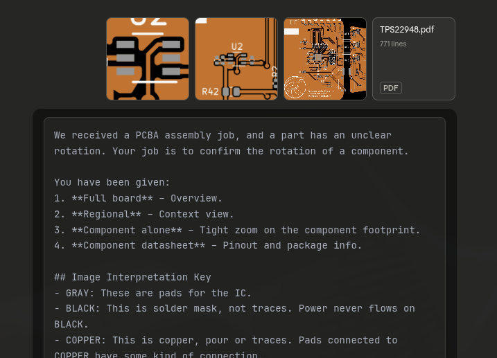
Automated Rotation Analysis
Determining Package Rotation
PCB assembly is putting a lot of parts in exactly the right spot every time. But the inputs to this process are inconsistent. Every design tool, PCB, and part has it's own idiosyncrasies. At Pikkolo, we focus on quick turn, low-volume assembly, so to do this effectively and at scale there's a lot of glue code between steps to standardize weird inputs.
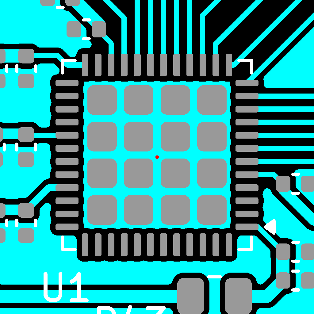
In this case, we needed a system to quickly figure out the rotation of an IC on a PCB.
Often this can be determine from the markings on the PCB, but in cases where it's unclear, we've built a system to automatically determine rotations from the copper alone.
(yes EE's, I realize it's pretty clear here, more below...)
{
  "reason": "Analyzed copper signatures against iCE40UP5K datasheet... <see post below>... The component is rotated 180 degrees.",


  "rotation": 180.0
}
Rotation 180!
We did it!

Rotations?
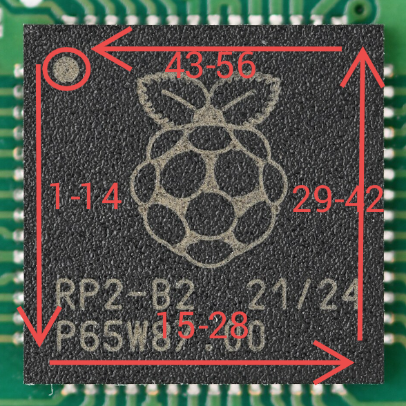
Parts need to be placed in the correct direction. Often there's a clear marking on the board, and sometime's it's not. And there are lot of different rotations going on at the same time:
Pin 1
If you're not familiar with electronics, integrated circuits (ICs) typically have a dot to indicate where Pin #1 is. There may be other markings, like a dash on the bottom.
Rotation 1: Feeder Sprockets
Tape feeds are covered by this the EIA-481 spec, linked here for bedtime reading.
For all it talks about tape feeds, it doesn't clarify if spocket holes should be on the left or right side of the tape. So there often a 180 degree rotation from the start.
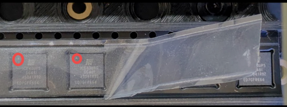
Rotation 2: IC in Tape
Convention for ICs within a tape feed is to orient such that it's orienting feature is facing the sprocket holes. That's the case with this FPGA:
But the spec doesn't really care how it's oriented otherwise:
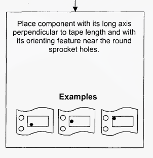
But it's also determined by geometry- a wider IC like an SOT-23 might be rotated to use a thinner tape.
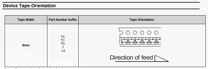
So, for safety we can never just assume how an IC will be oriented in the tape feed. It has to be checked for every part.
Rotation 3: Actual Part Rotation
The IC on the board can of course be rotated, often at 90-degree angles, but could be anything.
Rotations are counter-clockwise, so this RPI2040 above is rotated -90 degrees / +270 degrees.
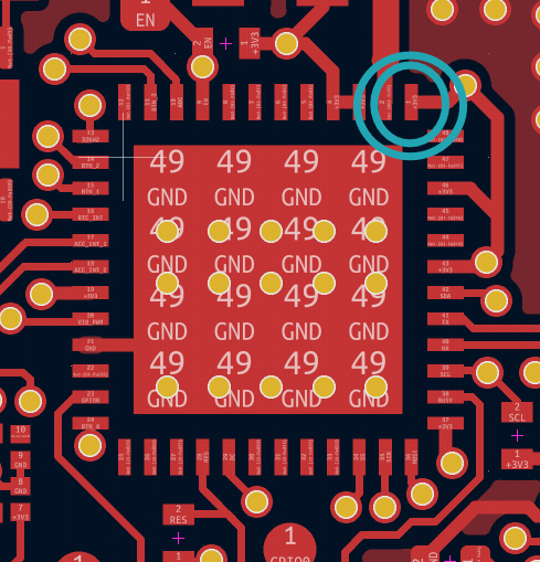
This is reflected in the pick-and-place file generated by the design tools. This file is used by the pick-and-place machine to put parts where they need to go:
U1     CD4060BM96    SOIC-16_3.9x9.9mm_P1.27mm     135.0000   -47.5000    90.0000  top
U2     MC14043BDR2G  SOIC-16_3.9x9.9mm_P1.27mm     134.9750   -58.4050     0.0000  top
These files- of course- come in a million different formats.
Rotation 4: Fabricator Plugins
But there's more! Some fabricators or users correct for these rotations.
For example, the Fabrication Toolkit KiCad plugin automatically applies rotations based on package to account for the above!
"Regex To Match","Rotation","Delta X","Delta Y"
"^Bosch_LGA-",90,0,0
"^CP_EIA-",180,0,0
"^CP_Elec_",180,0,0
"^C_Elec_",180,0,0
"^DFN-",270,0,0
"^DFN-",270,0,0
"^D_SOT-23",180,0,0
"^HTSSOP-",270,0,0
"^HTSSOP-",270,0,0
... and so on ...
So, even if we have everything aligned so far, a designer might export a position file that's applying rotations specific to some other assembly shop!
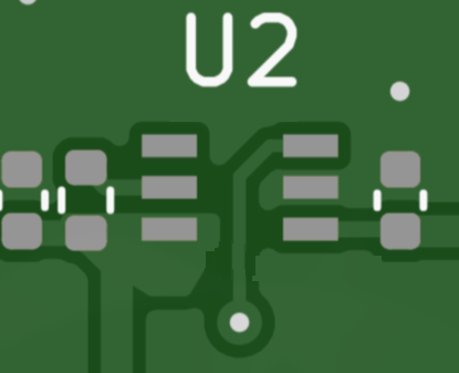
Can't You Use Silkscreen?
Yes, often this is obvious from the board itself, indicated on the silkscreen by a dot or notch pointing to Pin #1.

And sometimes it won't! A board may not indicate this. In this example, there's really no way to tell which direction the IC is oriented.
Result: Rotations are Effectively Random
Given this above- especially the fabricator-specific plugins- we need to double check our work without adding friction. Could we use an LLM?
Naive LLM Approach
Can a LLM to look at the pads, copper, and datasheet, and come figure it out?
As a first pass, I tried just dumping in images files and a datasheet:
This seemed so close to working, but not quite. The image is just too complicated, and every model I tried really struggled with left and right. I consistently got answers that were exactly inverted that no amount of prompting could resolve.
The good news is that LLMs are great at parsing pinouts from datasheets.
More Structure
So it seems like the image alone is a dead end. Can we provide structured data?
The standard file for PCBs are Gerber files, a format created in the 1960s. It works by defining apertures- like pen shapes- and dragging them around.
Here's an aperture for a round rectangle used for a pad:
G04 APERTURE LIST*
G04 Aperture macros list*
%AMRoundRect*
0 Rectangle with rounded corners*
0 $1 Rounding radius*
0 $2 $3 $4 $5 $6 $7 $8 $9 X,Y pos of 4 corners*
0 Add a 4 corners polygon primitive as box body*
4,1,4,$2,$3,$4,$5,$6,$7,$8,$9,$2,$3,0*
0 Add four circle primitives for the rounded corners*
1,1,$1+$1,$2,$3*
1,1,$1+$1,$4,$5*
1,1,$1+$1,$6,$7*
1,1,$1+$1,$8,$9*
0 Add four rect primitives between the rounded corners*
20,1,$1+$1,$2,$3,$4,$5,0*
20,1,$1+$1,$4,$5,$6,$7,0*
20,1,$1+$1,$6,$7,$8,$9,0*
20,1,$1+$1,$8,$9,$2,$3,0*%
... followed by commands to move the aperature around, stamping or drawing lines:
D15*
%TO.P,R11,1*%
%TO.N,VCCIO*%
X71800000Y-83810000D03*
%TO.P,R11,2*%
%TO.N,Net-(U2-FLT)*%
X71800000Y-82790000D03*
%TD*%
D16*
It not you, it's inscrutable. There's no way an LLM would make sense of this.
There's also an SVG image generated from Gerbers, which we can get from the awesome Tracespace project.
<circle
     cx="103015"
     cy="105235"
     r="135"
     id="circle2703"
     transform="scale(1,-1)"
     style="fill:#000000;stroke:#000000" />
  <polygon
     points="320,-135 320,135 50,135 50,-135 "
     id="polygon2703"
     transform="matrix(1,0,0,-1,103200,-105370)"
     style="fill:#000000;stroke:#000000" />
  <polygon
     points="185,0 -185,0 -185,270 185,270 "
     id="polygon2704"
     transform="matrix(1,0,0,-1,103200,-105370)"
     style="fill:#000000;stroke:#000000" />
Honestly not much better, a hundred thousand lines of XML.
Image Analysis
I needed to break the information down better, and understand what really is the key information to making a decision:
- Arrangement of pins
- What the pins are connected to
A good approach might be the amount of copper!
We'll start by generating an image from the board, centered on the component and some surrounding area.
Then, decode this image into a matrix to indicate PAD, COPPER, and EMPTY, eg:
[
  [EMPTY, EMPTY, COPPER, COPPER, PAD, PAD, COPPER, COPPER, ...],
  [EMPTY, COPPER, COPPER, COPPER, PAD, COPPER, EMPTY, COPPER, ...],
  ...
]
and in the process generate some really cool ASCII art:
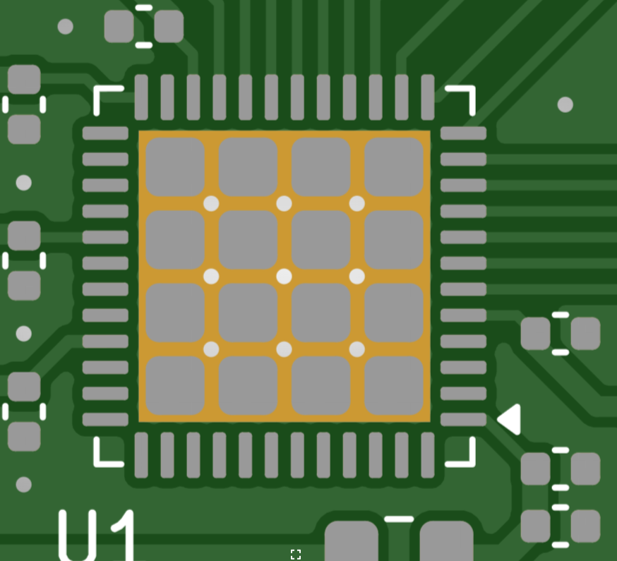
Next, we need to figure out which pads are actually part of the IC. There's probably an easy computer-vision solution here, but worked through it algorithmically, starting with the center point and expanding outward, collecting pads until symmetry breaks:
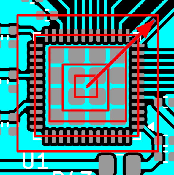
After we figured out which pads are part of the IC, we number them 1-N, starting in the top-left corner. To avoid confusion, we label these as pad_id instead of pin.
Then, for each pad, we flood-fill to count how many pixels of copper it's touching:

From this, we're able to get a relative list of how much copper the pad is touching:
{'position': (417, 449), 'copper_touching_pad': 0, 'side': 'top/left', 'pad_index': 1}
{'position': (417, 504), 'copper_touching_pad': 1102, 'side': 'left', 'pad_index': 2}
{'position': (417, 560), 'copper_touching_pad': 26362, 'side': 'bottom/left', 'pad_index': 3}
{'position': (605, 560), 'copper_touching_pad': 7391, 'side': 'bottom/right', 'pad_index': 4}
{'position': (605, 504), 'copper_touching_pad': 567894, 'side': 'right', 'pad_index': 5}
{'position': (605, 449), 'copper_touching_pad': 3030, 'side': 'top/left', 'pad_index': 6}
It's not perfect, does not show the full board, but starts to given an idea:
- Pad 1: No connection
- Pad 2: Connected to something
- Pad 3: Much larger connection
- Pad 4: Connected to something medium
- Pad 5: Connected to something HUGE!
- Pad 6: Connected to something
Looking at the pinout, the rotation becomes obvious:
- Pad 5 is probably a huge ground pour, mapping to Pin 2
- Pad 1 is not connected, mapping to N/C Pin 4

So this one is rotated 180 degrees.
Working!
I'll spare you the prompt, but it's effectively:
- Generate a pinout from the datasheet
- Look at the pads, and note copper amounts: N/C pads, adjacent pads with traces, and huge pours
- Rotate until it fits
The rotation trials could probably be done algorithimcally as well. But we now have a scalable system that can deduce package rotation directly from Gerber files and a datasheet.
{
  "reason": "Analyzed copper signatures against iCE40UP5K datasheet. \n\n1. **Power & Config (Left Side):** Datasheet defines Pin 5 (VCC), Pin 7 (CDONE), and Pin 8 (CRESET_B) on the Left side. These must be connected. The Observed data shows matching connections on the **Right** side at indices 29, 31, and 32 (corresponding to a 180-degree shift: 5->29, 7->31, 8->32).\n\n2. **PLL Power (Right Side):** Datasheet defines Pins 29 and 33 (VCCPLL) on the Right side. Observed data shows sparse connections on the **Left** side exactly at indices 5 and 9 (corresponding to 180-degree shift: 29->5, 33->9).\n\n3. **SPI Interface (Bottom Side):** Datasheet defines SPI pins (14-17) on the Bottom. Observed copper shows the Bottom side (pads 13-24) is completely unconnected, while the **Top** side (pads 37-48) has a solid block of connections matching the SPI group (Observed 38-41 maps to Datasheet 14-17).\n\n4. **Unused IO (Top Side):** Datasheet defines RGB/High-Current drivers on the Top. These map to the completely unconnected Observed Bottom side, which is physically plausible.\n\nConclusion: The component is rotated 180 degrees.",


  "rotation": 180.0
}
What's Next?
PCB assembly is a lot of extremely automated processes punctuated by tedious manual labor. Pikkolo's focus is low-volume, quick-turn jobs, so we want to remove as much manual labor as possible.
Running 1000 boards, it's reasonable for a human EE to validate each component. Running 5 boards, it's a lot more expensive.
Today, we're STILL going to have a human validate components. I consider this a proof-of-concept and a tool to assist an assembly tech until it's been proven out.